Embedded Components
Embedded Comopnents
Electronic devices are becoming smaller and smaller and must also be more powerful and reliable. This presents us with the challenge of developing innovative manufacturing methods. One method that can meet this challenge is embedded components.
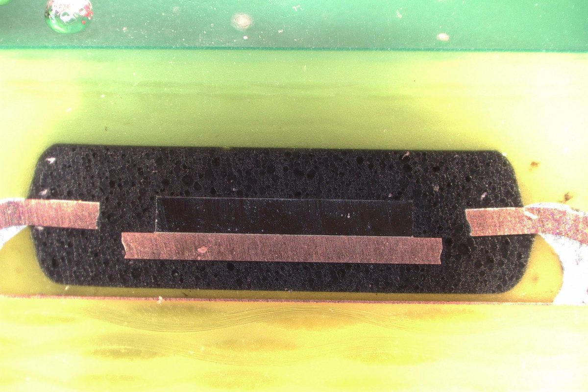
The idea behind this is fascinating: electronic components are no longer mounted on the surface of PCBs, but embedded directly in the PCB. This leads to impressive space savings, opens up new horizons for more compact designs and higher packing densities. But how does this work exactly?


There are three different methods to realise embedded components. Today we would like to introduce you to "solder embedding". This involves first making a thin inner layer to create a plane on which components can be soldered. Then a solder resist is applied around the solder pads like a frame. This reliably prevents the solder from flowing off along the tracks. The multilayer is layered with cut-outs in the prepregs, then pressed, completely filling the cavities. Further processing steps follow before the PCB is finally finished.
Why should you use embedded components? The advantages are manifold:
- Miniaturization: Savings in the assembly area on the outer layers of the PCB.
- Increased performance and improved functionality: Short signal paths and integrated shielding improve signal integrity and overall circuit performance.
- Reliability: Environmental protection and reduced mechanical stress for a more stable assembly.
- Efficient thermal management: Direct connection of the components to the copper plane of the PCB ensures effective heat dissipation, lower operating temperatures and longer service life.
plane of the PCB ensures effective heat dissipation,
lower operating temperatures and longer service life.
We are excited to see
how this technology will further change the world of electronics in the years to come.
What applications and innovations can you imagine?
