Micrograph analysis
Understanding the depth -
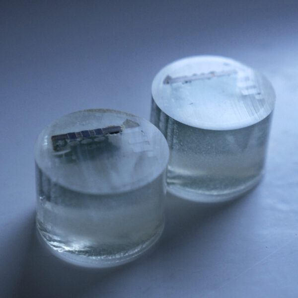
Micrograph analysis of PCB
Hidden behind the scenes of the electronics industry is a fascinating process - micrograph analysis of printed circuit boards. This technique gives us a fascinating insight into the world of printed circuit boards.
The micrograph analysis begins with a preparation process in which a cross-section of the PCB is embedded in resin. This block is then precisely ground until a perfectly flat surface is created. The final polishing gives it the finishing touch and ensures a flawless view. Depending on the requirements, a back-etching process can also be carried out.
Why is this process so crucial? Micrograph analysis plays a fundamental role in PCB quality assurance. It enables the detection of even the smallest defects, cracks, bubbles, delaminations and misalignments that would escape the naked eye. Particularly in sensitive applications such as medical technology, aerospace or the automotive industry, flawless PCBs are of utmost importance.
In a world where precision and reliability are top priorities, micrograph analysis is indispensable. It allows us to delve deep into the world of PCBs and ensure that they function smoothly and efficiently. A closer look beneath the surface can make all the difference between success and failure.